
We may be living on the cusp of an age of electronic clothes. There has been an impressive amount of research that may contribute to this reality, from conductors to power supplies that can be printed or deposited onto flexible surfaces like fabrics.
Many scientists envision that materials such as these will eventually be used to produce full devices that are thinner and lighter than ever before. These devices may be most useful for applications such as personal health tracking. They may also be used in novel displays, which could be interactive or user-controllable.
However, for this potential new tech to be useful or practical, they also need to be able to form fully integrated circuits, with transistors, gates and other components. Unfortunately, the materials that could support more two-dimensional circuits need to be able to form or be converted into inks for printing, and many have not responded well to attempts at this. However, the latest research that addresses this issue has resulted in a material that is printable, washable and functions as a transistor.
Flexible electronics
Flexible electronics are a part of our lives already, whether we realise it or not. Organic LEDs, some transistors and many photovoltaics are technically capable of bending and curving. However, they still often need to be integrated into rigid surfaces as the majority of consumer technology has not migrated to the use of fully-flexible circuitry and hardware yet.
However, there are materials out there that function as thin-layer circuits or components, and can even be laid down through deposition methods that even include printing. Therefore, they can be integrated into fabrics or textiles. These are capable of a number of interesting things, which include the conversion of movement or heat into energy, sensors and flexible antennae. Despite this, full two-dimensional circuits would require materials with a full panel of conductivity, dielectric properties and the ability to form active channels. Even though there are materials that do deliver all of the above, they often fail to stand up to the normal expectations of printed fabrics, which include the ability to be washed several times over. Therefore, they lose their circuit functions (e.g. field-effect transistor) as they degrade in response to use.
Most of these circuit-forming inks contain graphene, a powerful emerging conductor and semiconductor, and other compounds that confer properties such as insulation. These hybrid materials, known as heterostructures, have run into a variety of problems, the more common of which is the uncontrolled dispersion of electronically-active compounds in the presence of solvents. In addition, the concentration of some components in these hybrid materials occur at such low concentrations that they require multiple passes with the printer, thus resulting in thicker layers than the ideal (i.e. virtual or actual integration into clothes as normal inks or textiles).
In addition, some solvents included in early e-inks are toxic. However, a team from materials, physics, engineering, and graphene laboratories in Milan Polytechnic, Jiangnan University and Cambridge have developed a new ink that retained its field effect even after washing.
Wearable electronics need to withstand washing
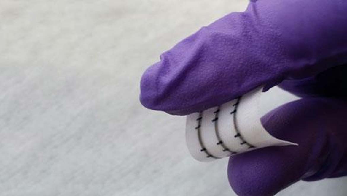
Their ink had a non-toxic solvent base with a lower boiling point (which forms more stable inks at room temperature) which contained graphene and nitrides of hexagonal boron (hBNs, which confer additional electronic properties). It could be deposited on polyester using drop-on-demand printing, which is a form of laser printing. It could achieve a field-effect mobility of approximately 91 cm2 per volt per second (cm2/V/s) at an operating voltage of <5 V. The researchers, who include Felice Torrisi of the Cambridge Graphene Centre, also found that the printed circuits could survive the equivalent of about 20 washes in a conventional machine.
The researchers started by printing their circuits onto coplanar PET in a test phase. They were able to print a transistor channel about 100nm thick using their graphene ink. They then added a source and drain made of silver ink (available from suppliers such as Sigma) of about 500nm in thickness, then a hBN gate with a top-gate made of silver ink on top of it. This resulted in a mobility of approximately 150 cm2/V/s. They then moved on to the polyester, which required modifications in the printing process to overcome the increased roughness of the surface the thin-layer circuits were to operate across. This involved coating the textile, which was a relatively slippery synthetic satin in any case, with a layer of polyurethane. Nevertheless, the increased roughness of this surface increased the resistance in graphene-ink channels (to about 40 megaohms), necessitating thicker layers. This, in turn, reduced the field-effect mobility. However, the team found that mounting the channel on a hBN dielectric layer gave a resistance of about 10 kilo-ohms. Therefore, they were able to keep the thickness of the channel to about 200nm.
The team also replaced the silver ink with polymers such as polyethylenedioxythiophene polystyrene sulphonate (PEDOT-PSS) at this point, as its ability to conform to the textile while still acting optimally as electronic components was improved compared to silver. The final circuits measured about 80µm in length, 500 µm in length and 200nm in depth. The researchers also claimed that their field-effect mobility was considerably superior to that achieved by other similar organic on-textile transistors (about 7 cm2/V/s at the most). The team also found that the mobility of their transistors could fall to as much as ~27 cm2/V/s in response to bending (when bent at a radius of up to 4mm). The circuits remained functional in response to 20 washing cycles, although the drain current fell from 94 to about 50 microamps. These new printable circuits could be used as logic inverters, complementary inverters, singular memory cells or a reprogrammable OR gate.
Circuits that can be printed onto or integrated into clothes are an ideal gateway to high-tech clothes are accessories for many researchers. This recent project, described in a paper published in Nature Communications, claims a breakthrough that results in the production of fully-printable, versatile and functional circuits that are nanometers thick, yet have low resistance. These circuits do not require metals or other materials that respond poorly to being printed or processed into thin-layer circuits. The team’s new transistors, which are graphene-rich and also have favourable dielectric properties, also appear to stand up well to being washed or flexed. Therefore, this article could be a turning point for an industry that specialised in ‘smart’ textiles or fabrics for many applications.
Top image: Fully integrated circuits printed directly onto fabric. Image source: (cam.ac.uk)
References:
- Carey T, Cacovich S, Divitini G, Ren J, Mansouri A, Kim JM, et al. (2017) Fully inkjet-printed two-dimensional material field-effect heterojunctions for wearable and textile electronics. Nature Communications. 8:(1). pp.1202.
- Collins S. Fully integrated circuits printed directly onto fabric. Cambridge Research News. 2017. Available at: http://www.cam.ac.uk/research/news/fully-integrated-circuits-printed-directly-onto-fabric


No comment