

Advances in nano-size materials promise to allow even smaller electronic products, and also with faster performance.
Smallest ever transistor
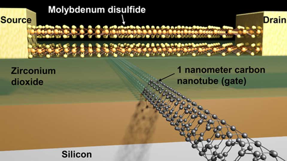
In October 2016, the journal science reported fabrication of the smallest ever field effect transistor (FET) using a single wall carbon nanotube only 1nm in diameter as the gate electrode only, crossing a zirconium dioxide insulator placed on a thin film of molybdenum disulfide as the semiconductor. The work was carried out by Professor Ali Javey and his team at the Lawrence Berkeley National Laboratory, run by the University of California, Berkeley under the Department of Energy.
Credit: Sujay Desai/UC Berkeley
This is remarkable, as usually a limit of 5 nm has been found before electrons, traveling from the source to the drain electrodes, ‘tunnel’ their way through the gate energy barrier. The significance is potential ability to reduce still further the geometry of present day silicon transistors to enable more compact integrated circuits for smaller electronic products. This would mean the maintenance of Gordon Moore’s Law: that the density of transistors doubles every two years.
Molybdenum disulfide is a compound semiconductor, whereas silicon is an elemental semiconductor. In the case of silicon there can be missing atoms known as atomic vacancies, but the usual way to get conductivity is by adding donor ions such as phosphorus or boron depending on the need for n- or p-type conductivity (where n-means conduction is dominated by electrons, p-means conduction is by hole, that is missing electrons). With semiconductors, dopants can also be used but naturally occurring vacancies can also contribute, especially for compound semiconductors. For silicon, a property of electrons called their effective mass is smaller than for molybdenum, so that tunneling occurs for shorter gate length and the transistor cannot be turned off. In addition, better control is possible for molybdenum disulfide due to its lower dielectric constant, a property that helps control the electric field, and its thinness of only 0.65 nm. In fact, molybdenum disulfide is a layered crystal, rather like graphite that is composed of carbon, and such layers easily slip over each other so that graphite and molybdenum disulfide are used elsewhere as lubricants. For these molybdenum disulfide transistors, just two atomic monolayers were obtained, and also of benefit was their uniform thickness.
Apart from the improvement due to use of molybdenum disulfide rather than silicon, using a carbon nanotube as the gate electrode avoided the difficulty of etching a metal to dimensions comparable to the wavelength of light where diffraction effects take place. These days, for the smallest of sizes possible with silicon, ultra violet light is used as having the shortest possible wavelength of light. This can achieve 20 nm geometry, although now improving to 5-10 nm. Thus, Samsung is said to have 14 nm geometry, and Global Foundries is aiming for 7 nm.
The team, measured on/off current ratios of about 106, which is extremely good, meaning little current is passed in the off condition.
Another candidate for the semiconductor function is graphene, where carbon atoms are also in a hexagonal array, but flat rather than folded up as tubes; again, this consists only one to four atomic layers thick. The most extraordinary features of these carbon structures are their very high electrical conductivity and strength.
Despite this apparent progress, the researchers cautioned that this had been merely proof of concept, and that achieving this repeatedly in production with high yield was yet to be shown.
Not only that, but one can imagine that picking out a single carbon nanotube from a possible tangle of them could be challenging. On the other hand, carbon nanotubes have been aligned as a forest of tubes for the purpose of emitting electrons as cathodes for backlights, with various methods, including an electric field, to do the aligning (much like aligning of liquid crystals in LCDs).
Speed Using just Carbon Nanotubes
Note too that carbon nanotubes just by themselves can function as electrodes, and even as transistors since they can be made metallic or into p- and n-type semiconductors. FETS can either p- or n-type as the semiconducting layer, in contrast to transistors that rely on a junction between p- and n-type.
Thus, Professor Michael Arnold at the University of Wisconsin-Madison published work on use of single-wall carbon nanotubes hailed as a breakthrough towards super-fast transistors predicted from properties of carbon nanotubes. Until now, carbon nanotubes transistors have not lived up to their promises of higher speed due to sorting, processing, alignment and contact issues. Instead, performance was some six times worse, but now the conductance is increased seven times, together with current density similar to that in silicon FETs, and greater than in gallium arsenide FETs. What’s more, this is with quite dense packing of 47 carbon nanotubes per micron.
Conclusion
Clearly, work on making transistors smaller or faster continues at a pace using new types of semiconductors or conductors. For carbon nanotubes, the commercialization of their robust nature has been underway for some time, such as mixing them in with polymers for car fenders, or as flexible transparent electrodes in displays, but taming their properties as transistors has lagged behind. This is due to the difficulties of separating out the various types of single versus multi-wall, or sorting the metallic forms from the p- or n- semiconducting type, and also depositing them in a dense pattern. Now, though there do seem to be some possibilities ahead. – Paul H.J. Beatty.
Top image: The view from inside a carbon nanotube. (CC BY-SA 3.0)


No comment