
Picture this: you’ve somehow come across a super-advanced, sophisticated crafting station from the far future. You can take components, including state-of-the-art semiconductors, and integrate them into devices to make fantastic high-tech equipment. Now imagine you’ve made a selection of quantum dots, silicon wafers and graphene to do just that. There may be many possibilities as to which gadgets this hypothetical combination may offer, but if you guessed that the actual result is ‘all-seeing camera’, you would…not be far wrong. In fact, a group of researchers in Barcelona have already proved that this is a concrete possibility.
CMOS and Graphene: Stronger Together?
Manufacturers in this reality have long known that you can use complementary metal-oxide semiconductors (CMOS) such as silicon to process and store data. CMOS applications can be found inside many familiar electronics such as computer processors, and also enable digital cameras to turn light that bounces off objects and passes through lenses into high-quality image files. However, stand-alone CMOS may have reached the upper limit of the technological power it can offer – unless it can be combined with other substances, including other semiconductor types, to move electrons around with even greater efficiency and flexibility. For example, graphene may have great potential as a new raw material for electronics, if it could act synergistically with silicon in order to do so. Whilst that might sound good in theory, these two conductor types have a history in research of not interacting well in close conjunction. Therefore, a research team from Barcelona set out to test a new way of combining these two materials. They then integrated quantum dots into their novel system in order to produce a sensor that can detect light in both visible and invisible ranges. The team collaborated across academic and industrial partner institutions: the Institut de Ciencies Fotoniques (the Institute of Photonic Sciences, or ICFO); the Catalonian Research Institute (ICREA) and the Spanish company Graphenea.
Multi-Material Sensors and Their Abilities
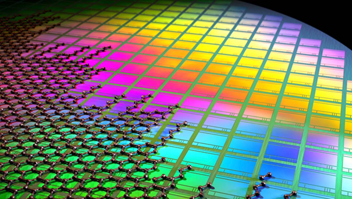
One of the most interesting features of the new IFCO system is that it combines three semiconductor types: silicon, graphene and quantum dots. They are arranged as a CMOS wafer, which is a common form of transistor array for processors, on which graphene is deposited. The research team, led by Frank Koppens of ICREA, solved the problems affecting graphene-CMOS integrations by first laying down the graphene and then shaping it into the optimal pattern for electron-transfer. Finally, a layer of lead-sulphide (PbS) quantum dots were laid down over the graphene.
ICREA - Welcome Frank Koppens! from Ondeuev Comunicación Visual on Vimeo.
PbS quantum dots are nanocrystalline colloidal semiconductors that can either emit or absorb light energy, also known as photons. In this case, the dots absorb photons and signal their presence by transferring electrons to the graphene layer. These electrons alter the conductivity of the graphene, which is in turn sensed by the rest of the array and converted to data. The entire multi-conductor system was installed into a digital camera, which resulted in the generation of high-quality image data that could ‘see’ a wide spectrum of light. This included wavelengths corresponding to visible light, ultraviolet and infra-red.
Advantages of Broad-band Sensors
A camera with a broad-band sensor which can detect light in this range has many potential uses. They can power dual daylight and night-vision cameras, which are a good feature to have in security equipment and for those studying zoological or environmental topics. Broad-band cameras that can see both visible and UV spectra may also enhance industrial safety systems, as well as many areas of science, medicine and food safety. The IFCO/ICREA/Graphenea team also claim that the method they have developed to combine CMOS and graphene does not require specialised conditions or processes, which has been a significant hurdle to the inclusion of graphene in modern micro-electronics. Koppens’ group also believes that this breakthrough will reduce the costs involved in producing these hybrid arrays, making broad-band optical sensors more ubiquitous over a shorter period of time.
Conclusion
Silicon is the CMOS basis for most electronic circuits in use today. They are capable of turning electrons that move across them into usable data for computers to process and store. Similarly, they can take photons that hit them or the sensors and convert them into workable image data. However, these circuits could be even more powerful if they could use a greater range of semiconductors. This would allow them to move and capture more charged particles in new ways, to detect light at wavelengths that can’t be seen by humans or existing machines. In other words, a combination of graphene and silicon on a chip might result in a sensor that can see both UV and IR light at once.
A team at IFCO have solved the issues that prevent graphene from integrating with CMOS to create more powerful processors. This has resulted in a light-activated transistor array that can ‘see’ light in a spectrum ranging from 300 to 2000 nanometers. This array, which also allows for the addition of a quantum dot layer over the graphene ‘pattern’, can absorb a wider band of photonic data compared to existing CMOS-only sensors. In other words, it can detect UV, IR and visible light at the same time. This has a range of interesting applications, from research to security concerns. It may also add high-tech new features to the camera modules found in phones and tablets. These exciting new transistor types may facilitate the availability of functions such as night vision into our everyday devices sooner rather than later.
Top image: Flagship researchers integrate graphene and quantum dots with CMOS technology to create an array of photodetectors, producing a high resolution image sensor. Image Credit: Fabien Vialla
References:
Goossens S, Navickaite G, Monasterio C, Gupta S, Piqueras JJ, Pérez R, et al. Broadband image sensor array based on graphene–CMOS integration. Nat Photon. 2017;11(6):366-71.
Crew, IT. Seeing The Invisible With A Graphene-CMOS Integrated Devices. Graphene Flagship. 2017. Available at: https://graphene-flagship.eu/graphene-cmos-integrated-devices


No comment