FinFET-based computer processors are one of the great breakthroughs of this age. Their form factors and architectures have allowed for the development of nearly every chip in nearly every device that enhance and sometimes define our lives today. Without these silicon microstructures, computerised gadgets as we know them might not have progressed to the relative power and portability they demonstrate as productivity and media-consumption tools. However, FinFET does have upper limits, particularly in terms of transistor density over a given area. Therefore, if computer processing is to get any stronger or more complex, processor architecture will inevitably have to move beyond this historical threshold and take on a new form. A collaborative effort between IBM, Samsung and other companies may have produced the next generation of transistors that will miniaturise processors beyond the traditional 7nm barrier.

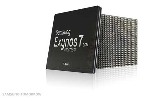
Samsung Announces Mass Production of Industry’s First 14nm FinFET Mobile Application Processor (CC BY-NC-SA 2.0)
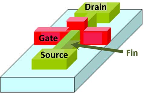
FinFET Structure and Some of its Functions
FinFET is the transistor standard that has revolutionised the form factors, computing abilities and power consumption of computer processors. It enables chips to have the small footprints we’re all familiar with, as well as their relatively astronomic electronic speeds that modern users take for granted. Without FinFET, consumer-grade electronics, particularly lighter and thinner device types including laptops and smartphones, simply could not exist. The transistors made based on FinFET architecture take the form of non-planar rectangles, or ‘fins’, of silicon atoms at the nanometric scale, stacked alongside one another. The fins can switch between states such as on or off very easily, while using ever-decreasing amounts of current at very high efficiency. This is the essential basis of modern data transfer and storage.

Schematic of a double-gated FinFET. By Irene Ringworm at the English language Wikipedia, (CC BY-SA 3.0)
The Limits of FinFET
Modern increments in processor speed and power depend on the steadily-increasing density and complexity levels at which the fins can be ‘stacked’. However, these properties inevitably meet ceilings, which are mainly determined by the atomic structure of silicon and the forces acting on it. This translates into a real-world limit of 5nm per FinFET-powered chip. However, because of other physical limits, mostly those of current flow between fins, these processors would be beaten by other form factors of a superior architecture on a chip of the same size. For example, silicon ‘fins’ are relatively static, which means they cannot adjust variably to the presence of current. Therefore, the best available FinFET-based processor units, or ‘nodes’, are about 10nm in size, whereas there is potential for more processing power per nanometer in the presence of improved silicon-based transistor types.
In other words, FinFET is still limited as to how many transistors can be packed into each nanometer of processor size. Currently, the best ratio that industrial research has produced equates to about 20 billion transistors across a 7nm node. This impressive array was developed by the Research Alliance, a consortium of investigators who have come together from major multinationals such as Samsung, GLOBALFOUNDRIES and IBM to assess the next directions for processing technology and how they may be realised. That was nearly two years ago, however. Currently, the Research Alliance has presented the debut of their new, 5nm node. This new device has increased the transistor number to 30 billion, and may represent the new generation of large-scale computing.
A New Variation on Transistor Arrangement
These new super-small chips imply the potential to pack a whole new level of semiconductor density into a single processing unit (which is arranged as layered nanosheets of silicon rather than complex ‘patterns’ of the material, as with FinFET). Chips made of these nanosheet-based nodes could carry hundreds of billions of individual transistors, allowing for an extremely high density of data storage or transfer. This super-high processing power is needed for applications such as cognitive computing (or the high-efficiency, high-speed completion of decision processes on which things like big data, machine learning and sophisticated AI depend), ‘cloud’ management and ‘internet of things’ control.
This sophisticated revolution in electronic ‘thinking’ depends on ultra-high-volume networks of data-transfer units that scientists ideally want to make resemble human neural networks as much as possible. Try as we might, these human neural networks are still more efficient and powerful than the most powerful computing arrays. To realise this, the industry would require processors carrying as many transistors as humanly possible. As FinFET is limited in the amount of electrons it can transfer over such small distances, these needs have officially moved beyond conventional technology. That’s where the new 5nm form factor comes in. These processors can also be made using the same manufacturing strategy developed for FinFET, known as extreme ultraviolet lithography. This involves ‘printing’ silicon onto a surface in the desired configuration, and has drastically reduced the cost and resources involved in producing the computer chips we all know today.

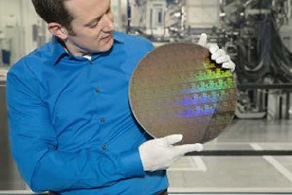
IBM Research scientist Nicolas Loubet holds a wafer of chips with 5nm silicon nanosheet transistors manufactured using an industry-first process that can deliver 40 percent performance enhancement at fixed power, or 75 percent power savings at matched performance. Press release link (Photo Credit: Connie Zhou)
FinFET vs. Nanosheet
The Research Alliance presented the work that led to the development of this new 5nm processor in a paper published in the proceedings of the 2017 symposium on very large scale integration (VLSI) based electronics. They claim that their chip can deliver 40 percent more performance when compared to the most advanced FinFET processor when both are running at the same power. The nanosheet-based processor can also reportedly save power consumption by 75 percent, compared to this FinFET chip under constant performance conditions. In addition, the paper’s authors point out that the nanosheets are much less complex to ‘print’ than FinFETs, thus possibly saving on manufacturing costs. This new processor type was developed by 64 Research Alliance scientists working at the NanoTech Complex, a facility associated with SUNY Polytechnic in Albany, New York. They propose the new silicon nano-layer technology as a viable successor to FinFET as the architecture of next-generation VLSI computing.
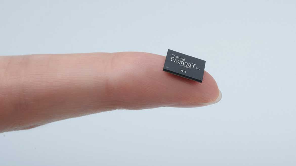
Top image: Samsung Mass Produces Industry’s First Application Processor for Wearable Devices Built on 14-Nanometer FinFET Technology (CC BY-NC-SA 2.0)
References:
Loubet N, Hook T, Montanini P, Yeung CW, Kanakasabapathy S, Guillom M, et al., editors. Stacked nanosheet gate-all-around transistor to enable scaling beyond FinFET. 2017 Symposium on VLSI Technology; 2017 5-8 June 2017.
Vu, C. IBM Research Alliance Builds New Transistor for 5nm Technology. IBM Newsroom. 2017. Available at: https://www-03.ibm.com/press/us/en/pressrelease/52531.wss
Bu, H. 5 nanometer transistors inching their way into chips. IBM ThinkBlog. 2017. Available at: https://www.ibm.com/blogs/think/2017/06/5-nanometer-transistors/


No comment