Nanowires are short, thin rods of material such as gallium arsenide that are present at the sub-micrometric scale.
They are grown on substrates such as silicon wafers in a way that resembles molecular self-assembly. Understanding this process is also key to controlling and modulating it. These abilities would mean scientists could create their own custom nanowires, which could be beneficial to numerous areas of science and technology.
A difficult process
However, the accurate observation and monitoring of nanowire growth has proven difficult. It seems that a specially-designed apparatus for use in the German Electron Synchrotron (DESY) is necessary to do so. The results of just such a project were published in the journal Nano Letters.
This study was conducted at the Karlsruhe Institute of Technology (KIT), which houses DESY and, accordingly, facilitates a lot of particle physics research. The researchers involved were affiliated with KIT, the University of Siegen or the University of Hamburg.
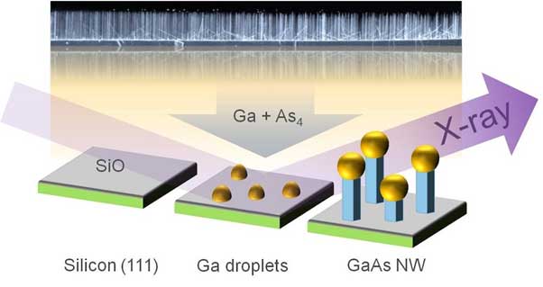
The team developed an experiment in which the formation of gallium-arsenic (GaAs) nanowires was tracked using in situ structure analysis and ex situ electron microscopy. The in situ characterisation was enhanced using X-ray beams supplied by the PETRA III component of the synchrotron. It was captured in a portable module that was custom-designed at the Institute for Photon Science and Synchrotron Radiation within KIT.
This module housed the apparatus for GaAs nanowire manufacture. This process depends on the deposition of liquid gallium onto a silicon wafer heated to approximately 600⁰C. The gallium forms tiny droplets on this surface, which is then bombarded with atoms of both gallium and arsenic.
The results of this technique, known as vapor-liquid-solid (VLS) process, are nanowires of the compound gallium arsenide, which form underneath the droplets. This is what is known about VLS; however, little is known about the variables of nanowire formation that could be harnessed for improved control of the VLS process. Therefore, the module was set up under the light from PETRA III to record this activity.
New discoveries
The scientists found that nanowire formation is determined by two distinct factors: those of gallium droplet size and side-wall formation. The latter of these, which was not really anticipated by the researchers, determines the width of the complete nanowire, and is influenced by radial growth. The researchers also found that the gallium droplets increase in size during VLS. This is due to their augmentation by the gallium atom bombardment. However, this means that the angle at which the droplet touches a growing nanowire can change over time. The scientists reported that these variables could result in different structure types within the same nanowire.
This is bad news for scientists who may need more uniform nanowires for their research. On the other hand, this study may lead to more sophisticated VLC processes that avoid changing the droplet size, and, thus, varying the manner in which the crystals grow. In addition, the scientists found that crystal length over time was influenced by contact angle. The upward nanowire growth (measured in nanometres) experienced an overall increase as the angle dropped.
Gallium arsenide is a useful semiconductor that is used in many conventional electronics and devices (e.g. remote controls for televisions). It is also used in solar energy capture devices for extraterrestrial vehicles or stations. Nanowires of the material are used in imaging studies that improve the study of phenomena such as phase-reaction dynamics. For example, they have been used in four-dimensional EM studies of what happens to gallium arsenide when it melts. Therefore, their production could be important to research or development scientists in these areas.
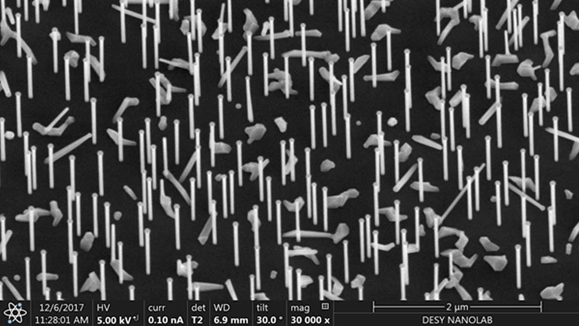
Small thin nanowires grow on a silicon wafer after bombardment of gallium droplets with gallium and arsenic. Growth can be monitored with the help of X-rays. The fully grown nanowires were examined by electron microscopy (background). (Figure: Philipp Schroth, KIT)
In other words, this study of the VLS process is useful as it has uncovered some possible flaws of the technique. It has revealed that the droplets of liquid gallium are subject to variation in the course of the process. This, in turn, can change the structure of a nanowire part-way through its manufacture. Compromising the nanowire structure may inadvertently lead to impaired data-collection in studies of their physical properties. Therefore, the scientists at KIT may have found out more than they anticipated when designing their experiment.
The results of this study, which have been recently published in the journal Nano Letters, also generally demonstrates that it is possible to observe and track a process such as VLS… so long as you have a synchrotron handy. This may be relevant to other scientists who aim to study the effects of extreme conditions (such as those in space, an environment in which gallium arsenide makes up solar panels) on the material in question. The research conducted at KIT may also lead to a greater understanding of how to control nanowire formation in situ, so as to improve on or diverge from their current structure.
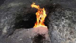
Top image: Nanowires on a silicon wafer as recorded at the DESY NanoLab. (Photo: DESY, Satishkumar Kulkarni/Thomas Keller)
References
Schroth P, Jakob J, Feigl L, Mostafavi Kashani SM, Vogel J, Strempfer J, et al. Radial Growth of Self-Catalyzed GaAs Nanowires and the Evolution of the Liquid Ga-Droplet Studied by Time-Resolved in Situ X-ray Diffraction. Nano Letters. 2018;18(1):101-8.
Chen B, Fu X, Tang J, Lysevych M, Tan HH, Jagadish C, et al. Dynamics and control of gold-encapped gallium arsenide nanowires imaged by 4D electron microscopy. Proceedings of the National Academy of Sciences. 2017;114(49):12876-81.
Landgraf M. Scientists Observe Nanowires as They Grow. KIT News. 2018. Available at: https://www.kit.edu/kit/english/pi_2018_010_scientists-observe-nanowires-as-they-grow.php


No comment