
Graphene is a fascinating and relatively novel material that may have a whole range of applications in the areas of electronics and engineering in the near future. It is a superconductor that has recently demonstrated the ability to co-exist with silicon to enhance the capabilities of this complementary metal-oxide-semiconductor (CMOS). These capabilities include photonics: for example, silicon/graphene transistors have recently formed the basis of a sensor that can ‘see’ visible, IR and UV light simultaneously. On the other hand, the properties of graphene are not as well understood as those of silicon are. This is currently an enduring barrier to its more widespread use in electronics. However, a team from Australia may have developed an imaging system that can visualise the electron-transport system within graphene that is based on the material’s own specific properties and attributes. This may help scientists to broaden their understanding of how information transfer across graphene can work, and how it may be exploited to produce new transistors with enhanced specifications and processing power.
The many properties of graphene
Graphene can exist as a sheet of just one atom in depth, and yet it is super-strong and conductive. It is also flexible and see-through, thus expanding its use-cases to display, solar-power harvesting and ultra-thin circuit technology. These potential functions offer industrial designers new options in terms of the durability, weight and ergonomics of future devices. On the other hand, the behaviour and movement of electrons within graphene has not been investigated thoroughly enough to enable scientists to design transistors and other circuit elements using the material, as the current flowing through them may not be as predictable as needed to optimise their form and function. This is a shame, particularly as graphene has obvious advantages as the material from which quantum computers could be built. Graphene is also cheap to manufacture, as it is composed nearly entirely of carbon, after all. Therefore, its use in quantum computing could accelerate the affordability and ubiquity of this new processing standard that is promised.
Unfortunately, the use of conventional techniques that quantify current across materials is often not entirely satisfactory when applied to graphene. They are often too ‘invasive’ in terms of the material’s structure, thus biasing and skewing the results. Alternatively, studies that elicit the electron transport across graphene may offer models of these interesting properties based on perfect, laboratory-grade samples of the substance (e.g. resisitivity-based techniques that ‘flatten out’ the spatial profile of electron flow), and not how they manifest in real-world scenarios and materials (which would have tiny flaws, defects and edges that would alter conductivity in their region of the graphene sheet). A more effective method of graphene evaluation would involve techniques that are more relatable to medical imaging, in which the experimental intervention is derived from the natural feedback of the atoms in graphene. A team of scientists from the University of Melbourne in Australia may have done just this, using a well-known property of carbon lattices such as graphene: the ‘colour centre’.
The Colour Centre
The ‘colour centre’ is found in ordered carbon structures that include diamonds and graphene. It has been observed to absorb light of one particular frequency to emit the light of another. This occurs as a result of mono-atomic impurities in carbon lattices – in other words, an atom of nitrogen has somehow found its way into a space that should be taken by just another carbon atom. These nanoscopic anomalies, known as nitrogen vacancies or NVs, in carbon lattices can be exploited to elicit changes in electron spin and energy states, and also emit red light when green light is shone on them. The Australian team, led by Professor Lloyd Hollenberg at Melbourne’s School of Physics, integrated the latter into a quantum probe array that could visualise the magnetic field, and thus the spatial arrangement of current distribution, across graphene.
The team were able to visualise changes in the density of electron-flow across narrow sheets, or ribbons, of graphene, as well as those changes at graphene/metal junctions. These were deposited onto a diamond chip with a consistent layer of NVs to form a quantum photoluminescence-based array. The changes in photoluminescence corresponded to the graphene’s magnetic resonance in response to current (at +0.8 mA) injected into the material. The resulting data was converted to photoluminescence images, optically detected magnetic resonance spectra and vector-density maps. The vectors had a precision that equated to 5 percent, and the density had a sensitivity of 1A/m, meaning that one microamp could be detected across one micrometre of graphene.
The array could also be imaged using scanning electron microscopy (SEM), which captures images with features of up to 200nm in size. These images showed how tiny irregularities in the graphene ribbon’s structure gave rise to sizeable (in nanoscopic terms) and proportional disruptions in the density of the current. These irregularities are defects caused by conventional graphene-production and deposition processes. Interestingly, there were also observable variations in regions that were completely free of these defects. Their pattern suggested that current is most dense at the centre of a graphene sheet, and that it gets more diffuse towards the edges. The images of the junctions between graphene and metal (titanium-gold electrodes) showed that current drops off at this interface, possibly because the graphene is torn as it is fitted around electrodes, and because the current density is reacting to differences in width or depth between metallic contacts and graphene.
This University of Melbourne project offers a new, non-invasive (the NV layer was about 20nm below the diamond’s surface, thus negating the problems and current loss direct contact between array and graphene may have posed) imaging modality to assess electron flow across graphene. The study may offer helpful tips to bodies who are preparing to manufacture graphene for circuits, the most prominent of which is that their process needs to result in high-quality, low-defect sheets for optimal conduction. Alternatively, micro-defects in graphene could be exploited for interesting forays into current modulation or other favourable electronic properties. The study at Melbourne also highlights the fact that metallic contacts may cause issues in graphene-based circuits. This work and its future directions may be what guides and informs the use of graphene in the upcoming generations of processors and quantum computers.
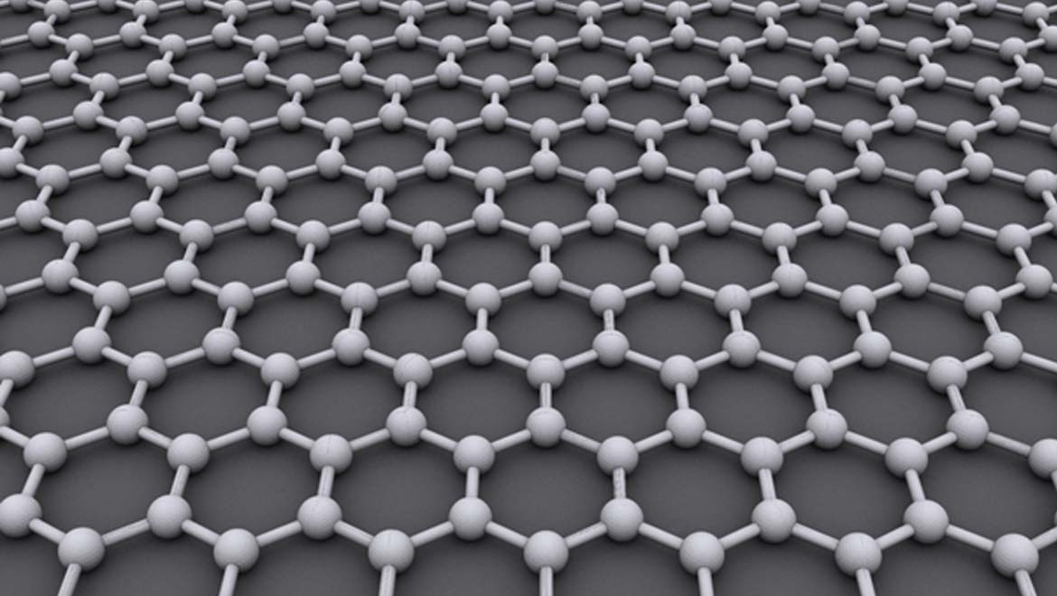
Top image: Graphene is an atomic-scale hexagonal lattice made of carbon atoms. (CC BY-SA 3.0)
References:
Tetienne J-P, Dontschuk N, Broadway DA, Stacey A, Simpson DA, Hollenberg LCL. Quantum imaging of current flow in graphene. Science Advances. 2017;3(4).
Hannick, N. Seeing The Electricity Inside Graphene For The First Time. Pursuit. 2017. Available at: https://pursuit.unimelb.edu.au/articles/seeing-the-electricity-inside-graphene-for-the-first-time/


No comment