
If they were asked to think of a material to make solar cells, professionals might be inclined to think of perovskite - a mineral strongly associated with photovoltaics or electronics that are activated by light or store it in the form of energy (mostly as sunlight).
However, silicon has also enjoyed a great deal of success in this arena. Photovoltaics based on this element can stretch to 30% or more, efficiency-wise. Therefore, silicon constitutes about 90% of the solar cell market. But this material is also reaching its limits, in terms of what it can bring to solar power conversion.
Advantages and Disadvantages of Hybrid Photocells
Some scientists believe that this may be addressed by counting perovskite back into these devices. This results in a device known as a silicon/perovskite double junction.
These products may be particularly advantageous as the resulting photovoltaic device could capture the light of a broader spectrum. Perovskite tends to absorb light of blue to green wavelengths, whereas silicon absorbs those associated with red to infra-red.
However, this potential solution for increased efficiency is fraught with drawbacks. The silicon in these junctions needs to be covered with the perovskite in order to exploit this full-spectrum light capture. This also means that the silicon needs to be highly polished to be compatible with conventional perovskite deposition techniques.
Smooth, shiny silicon surfaces pose a huge detriment to solar cell efficiency. They make the entire surface much more reflective because of which a large amount of radiative energy evades absorption by bouncing away. Polishing adds to the costs involved in hybrid solar cell production. This additional step damages the appeal of solar power through lost cost-effectiveness and more complex industrial processes.
On the other hand, double junctions are among the more feasible and plausible options to drive overall cell efficiency above the 30% mark.
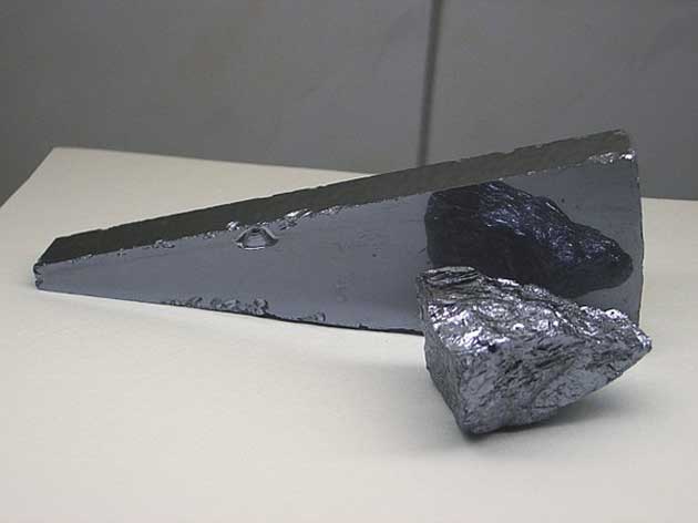
The shiny silicon (in this picture) has been observed, through past research, to be less than optimal for inclusion in a photovoltaic cell. (Source: W. Oelen @ Wikimedia Commons)
Reinventing the Double Junction
A team of scientists from the Institute of Microengineering at the Lausanne Federal Polytechnic School, in conjunction with others at the Swiss Center for Electronics and Microtechnology in Neuchatel, Switzerland, believe that they may have overcome the above problem.
The team has reported on their novel process to produce double junctions in a recent paper in the journal, Nature Materials. The study included a top cell-type deposition process that could induce inorganic nano-complexes to form on a surface of unpolished silicon.
This process allowed for the successful deposition of liquid perovskite (as in the production of other double junctions). Therefore, the need to polish the silicon is eliminated, and the desired double-junction is formed.
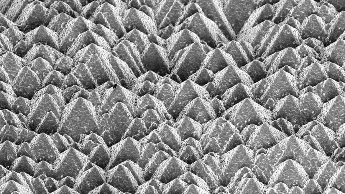
This new technique has a number of advantages: One, it allows for conventional perovskite-deposition steps such as spin-coating, which may keep manufacturing costs under control. Two, the method enables the silicon layer to retain its normal conformation, which is a pattern of raised and pointed pyramids at the micrometric scale. Therefore, the total surface area available to sunlight is enhanced, and the reflectivity of the cell may be limited.
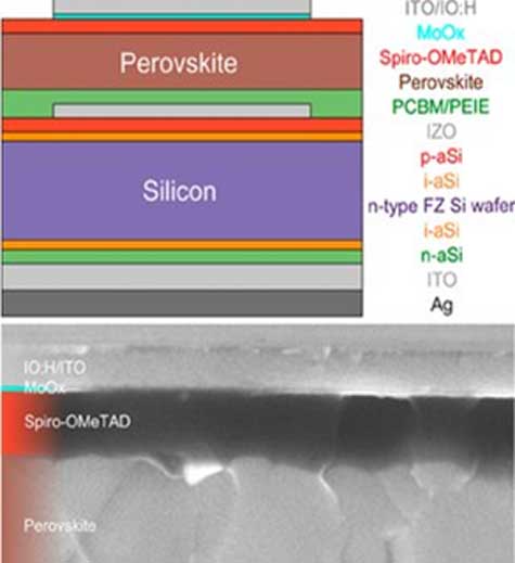
Illustration of planar monolithic double junction (perovskite/silicon) solar cell. (Source: Werner, J. EPFL)
The Neuchatel researchers also reported the presence of a silicon hybrid junction, as well as a recombinant silicon junction, within their newly-created cells. This setup exhibited an efficiency of just over 25% at a steady state, as well as a current density of 19.5 milliamperes per centimeter.
The researchers attributed these impressive results to the retention of the silicon micro-texture. They also asserted that further refinements of this device could lead to the magic 30% efficiency figure.
Conclusion
All in all, this study has highlighted the importance of a ‘raw’ silicon surface to photovoltaic cell efficiency.
The Swiss researchers say that the current trend towards polishing diminishes the optoelectronic properties of the material, which, in turn, decreases overall efficiency. Therefore, the removal of the polishing step may be extremely beneficial to the photovoltaics industry, even if another is added in its place.
Furthermore, the organic base layer leads to baking the liquid perovskite on top of it until it forms a crystalline layer. However, the temperature needed to do so is around 150⁰C, which is relatively low in manufacturing terms.
This research may be the key that unlocks the door to relatively super-efficient – and cost-effective – photovoltaic cells.
The hybrid device developed as a result also allows a photovoltaic cell to exploit the optoelectronic advantages of both perovskite and silicon. This innovation, in the future, could be converted into an important incentive for the improved uptake and use of solar power.
Top Image: Scanning electron microscope-generated image of the silicon micro-pyramids coated with perovskite. (Source: EPFL)
References
F. Sahli, et al. (2018) Fully textured monolithic perovskite/silicon tandem solar cells with 25.2% power conversion efficiency. Nature Materials.
Solar cells combining silicon with perovskite have achieved record efficiency of 25.2 percent, 2018, Eurekalert, https://www.eurekalert.org/pub_releases/2018-06/epfd-scc061118.php , (accessed 12 Jun. 18)
New Developments in Solar Cell Components May Offer Improved Photovoltaics, 2018, Evolving Science, https://www.evolving-science.com/environment/new-developments-solar-cell-components-may-offer-improved-photovoltaics-00553 , (accessed on 12 Jun. 18)


No comment